From Microscopy to Manufacturing: Top 6 Cutting-Edge Ultrafast Laser Applications

Ultrafast lasers are transforming science and industry. Here, we present six groundbreaking applications enabled by Class 5 Photonics high-power femtosecond lasers: attomicroscopy, high-speed brain imaging, compact particle accelerators, EUV metrology, time-resolved ARPES, and advanced nanolithography.
At the forefront, Class 5 Photonics delivers high-precision laser systems that enable researchers and engineers to push the boundaries of discovery. Whether refining imaging techniques or revolutionizing manufacturing, ultrafast lasers are unlocking new possibilities.
In this blog, we’ll uncover how these powerful lasers are driving the next wave of scientific breakthroughs. Whether you’re a researcher, engineer, or technology enthusiast, join us as we delve into six cutting-edge applications that are redefining the future of science and innovation.
1. Functional brain imaging using 2-photon multiplexed sculpted light microscopy
Advanced multi-photon microscopy enables non-invasive imaging of deep cellular structures, enabling breakthroughs in neuroscience and cancer research. Calcium imaging with two-photon microscopy is vital in neuroscience, but traditional methods face trade-offs in the fields of view, speed, and depth. One approach introduces a new design paradigm that allows real-time 3- dimensional imaging of neuroactivity in a large volume. It uses hybrid multi-photon acquisition for high-fidelity volumetric recordings at single-cell resolution within 1 × 1 × 1.22 mm³ volumes at up to 17 Hz in awake mice. The imaging system captures neuroactivity in the mouse auditory cortex, posterior parietal cortex, and hippocampus, demonstrating its ability to record up to 12,000 neurons, revealing the system’s versatility and potential for in-depth brain studies.
Check the article here https://www.cell.com/cell/fulltext/S0092-8674(19)30273-9
Video S2. Example 4× Axial Recording of Mouse neuronal activity. 3D rendering of a 30min volumetric recording in a volume of 690 × 675 × 600μm, 16.7Hz frame-rate, using a cytosolic GCaMP6f genetic calcium marker. The video shows the first 3min of the recording (Playback speed: 3 ×)
|
Laser used: |
 |
White Dwarf hybrid |
|
|
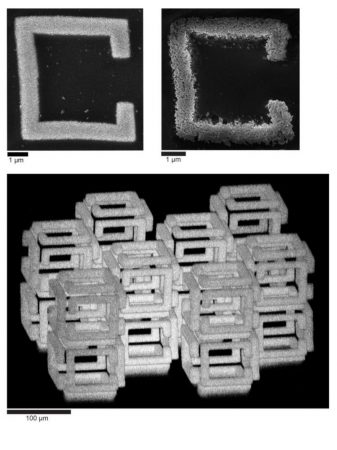
2. Scaling maskless 3D nanolithography via TPA
Two-photon polymerization (TPP) nanolithography is an advanced fabrication technique used to create highly precise three-dimensional (3D) micro- and nanostructures. The process relies on a nonlinear optical effect (two-photon absorption) in which a photosensitive material, typically a liquid resin, undergoes polymerization only at the focal point of a tightly focused femtosecond laser beam. It occurs when two photons of lower energy are simultaneously absorbed by the resin to trigger the photochemical reaction.
The unique feature of TPP is its spatial resolution, which can achieve feature sizes smaller than the wavelength of the laser used, thanks to the confined nature of the two-photon absorption process. This makes it possible to construct complex 3D structures with nanoscale precision.
We offer high power and high repetition rate Laser solutions in an industrial one-box design to multiplex and parallelize TPP. This paves the way for highly scalable 3D Nanolithography production lines which will be able to compete with classical lithography approaches.
|
Class 5 Product recommendation: |
 |
White Dwarf TPA |
|
|
3. Complete beamlines for time-resolved ARPES
Time-resolved angle-resolved photoemission spectroscopy (tr-ARPES) is an experimental technique that combines the spatial and momentum-resolved detail of ARPES with the time resolution of ultrafast laser pulses. By exciting a sample with a short VIS or NIR “pump” pulse and subsequently probing the excited sample with an EUV “probe” pulse, researchers can track how electronic structures evolve on femtosecond timescales. This is particularly valuable in materials science because it provides direct insight into transient states, electron correlations, and ultrafast processes—such as charge dynamics and phase transitions—helping researchers understand, and potentially engineer, novel electronic and optical properties. We offer complete tr-ARPES beamline solutions within our Moonlander HHG series and tailor the beamlines to your specific requirements.
Check the article here: https://www.nature.com/articles/nphys3609#citeas

|
Class 5 Product recommendation: |
| Moonlander HHG-21.7 | |
|
|
4. Soft X-ray scatterometry for semiconductor device metrology
High-harmonic generation (HHG) sources provide all the desired quality parameters for at-resolution metrology and inspection tools required in state-of-the art EUV lithography: Their coherent radiation at few-nanometer wavelengths match the scale of modern 3-dimensional EUV-fabricated nanodevices, such as gate-all-around (GAA) transistors. EUV and soft-X-ray (SXR) scatterometry and lens-less imaging with broadband, high brightness HHG sources enables mask inspection and device metrology with sub-100 µm focal volumes, revealing geometry, material contrast and depth information with highest precision within seconds.
Check the article here: https://www.spiedigitallibrary.org/conference-proceedings-of-spie/12496/124961I/Soft-x-ray[…]rology-for-3D-profilometry-and/10.1117/12.2658495.short

|
Class 5 Product recommendation: |
| Moonlander HHG-50 | |
|
|
5. Attomicroscopy
Attomicroscopy facilitates direct observation and imaging of electron dynamics in real-time and space, enabling unprecedented insights into the structural and electronic dynamics of materials at the quantum level. It achieves attosecond temporal resolution within transmission electron microscopes (TEM) by combining them with powerful femtosecond lasers. The developed methodology combines attosecond optical gating with a polarization-gated half-cycle laser pulse to generate single attosecond electron pulses within the TEM. These pulses allowed researchers to probe field-driven electron dynamics in multilayer crystalline graphene through attosecond electron diffraction. Attomicroscopy bridges the gap between attosecond time resolution and atomic spatial resolution imaging.
Check the article here https://www.science.org/doi/10.1126/sciadv.adp5805

|
Laser used: |
| Supernova SN-800 | |
|
|
6. Coherent nanophotonic electron accelerator
Particle accelerators play a crucial role in science, industry, and medicine, but they are typically very large and expensive facilities. A promising alternative is using ultrashort laser pulses to accelerate electrons within nanophotonic structures, which would significantly reduce size and costs. This research demonstrates a scalable nanophotonic electron accelerator that coherently combines particle acceleration and transverse beam confinement, and accelerates and guides electrons over a considerable distance of 500 μm in a just 225-nm-wide channel. It achieves a 43% energy increase from 28.4 keV to 40.7 keV and therefore, marks a breakthrough in nanophotonic electron accelerators. These findings could pave the way for compact, high-gradient accelerators up to the GeV m range.
Check the article here https://www.science.org/doi/10.1126/sciadv.adp5805

|
Laser used: |
 |
White Dwarf HE |
|
|
Class 5 Photonics is proud to contribute to this progress with our high-precision laser solutions, empowering researchers and innovators worldwide. We look forward to supporting even more pioneering discoveries that continue to push the boundaries of science and technology. Stay tuned, the next publications are already on the way.


